Welcome to
ChipInventor
Cloud based EDA platform
Beta Version
What happens when anyone, anywhere, can become a ChipInventor?
WHAT IS CHIPINVENTOR?
ChipInventor is an innovative, cloud-based EDA (Electronic Design Automation) platform, currently available in its beta version.
It is designed to democratize semiconductor development by leveraging open-source tools and proprietary technology, making chip design accessible to all.
At this moment, we offer practical learning Journeys that introduce fundamental design concepts. These experiences are granted via vouchers, which can be requested for access to the platform.
Frontend DesignBackend Design3D Layout ViewerFoundry AccessRISC-V Ready
Partners:

JOURNEY
A hands-on learning journey with VBAcademy
using the ChipInventor platform.
Learn semiconductor design from basics to complete Chip flow with AI-powered support.
using the ChipInventor platform.
Learn semiconductor design from basics to complete Chip flow with AI-powered support.
FROM DESIGN TO SILICON
Our platform is your cloud-based path to custom chip fabrication, offering a unique opportunity to transform your final project into a real silicon device. This integrated approach provides highly cost-effective prototyping at a fraction of the industry standard price.
Go beyond simulation: ChipInventor provides expertise in wafer preparation and packaging, allowing us to deliver ready-to-use components.
This optional add-on for Journey participants handles the entire tapeout process, letting you focus exclusively on your design.
Go beyond simulation: ChipInventor provides expertise in wafer preparation and packaging, allowing us to deliver ready-to-use components.
This optional add-on for Journey participants handles the entire tapeout process, letting you focus exclusively on your design.
Take your project beyond simulationFull tapeout flow on a real foundryDelivery of your design as manufactured silicon
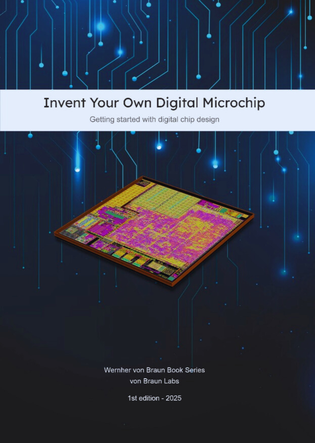
OUR EBOOK: INVENT YOUR OWN DIGITAL MICROCHIP
Discover the fundamentals of digital microchip design in a practical and accessible way.
This ebook guides you through the essential concepts of logic, architecture, and implementation — empowering you to create and understand your own digital circuits.
Perfect for students, makers, and aspiring chip designers.
This ebook guides you through the essential concepts of logic, architecture, and implementation — empowering you to create and understand your own digital circuits.
Perfect for students, makers, and aspiring chip designers.